
BeforeHand addresses the specific challenge of developing a new generation of Electronic Smart Systems (ESS) technology with focus on advanced functionalities such as processing/storage with improved reliability and reduced power consumption leading eventually to costs reduction.
Nowadays the demand for processing/storage products is much broader, mainly because of the rising appetite in the mobile sector. Sales of new smart phones and tablets boosted and, in addition, modern mobile devices require, for example, much more memory than previous ones. Before 2008, the memory market primarily depended on sales of PCs. Today, the need for data centers for Internet and cloud applications increased and is further growing rapidly. Among others, one technology, the Internet of Things (IoT), drives promise for such impressive long-term growth.
IoT refers to a giant network of connections centered on providing distributed intelligence, sensing and connectivity to ESS around us. Such a scenario is no longer the wave of the future; it is here right now and is growing quickly. The IoT is connecting people, places and ESS at a rapid pace. It is a concept that not only has the potential to impact how people live and work, but also how the human society is managing its resources. IoT certainly opens the door to a lot of opportunities, yet bears many challenges. With the surge of connected ESS comes the demand and necessity to implement the exchange and processing, as well as the storage of all the data. The explosion of information that ESS devices within IoT will gather will require huge numbers of low-cost, secure and reliable embedded, non-volatile memory (NVM) for several storage and/or advanced processing purposes. A special societal impact of IoT is given by automotive applications, as related to infotainment, safety and fuel efficiency. For this application an important requirement is that the ESS must be reliably working at a temperature of 165°C. In this respect not all technologies are reliable.
One of the most promising NVM is based on PCMs. PCMs were the heart of optical storage technologies, where data was encoded using the material’s phases. Amorphous and crystalline phases display strong optical contrast along with fast and reversible switching between those two states. As this large variation in optical reflectivity between the amorphous and crystalline state is accompanied by a huge difference in resistivity (up to six orders of magnitude), PCM play a revolutionary role also in microelectronics.
 BeforeHand aims at realizing chalcogenide heterostructures, aiming to provide a processing/storage, all-in-one device, to be embedded in automotive IoT smart devices.
Why using chalcogenide multilayers?
The basic idea is to create multilayers of chalcogenides of different alloy and compound combinations. The PCM cell takes advantage of the merits of the different sorts of materials used for the stack. To be more concrete, let us consider to choose a material with the ability to enhance the write speed (reduce the latency); then it must have a high crystallization speed. However, such materials often suffer from poor thermal stability (low retention). The dilemma between speed and stability is in practice solved by sacrificing the speed to assure the cell thermal stability. In recent time, research on superlattice structures of alternating Sb2Te3 and GeTe or GST revealed not only higher speed than GST, but also a better thermal stability than Sb2Te3 films is expected, although an experimental verification is missing. This shows that combining layers of materials with different physical properties might help to achieve the best material trade-off.
Here we aim at designing unusual active storage/processing layers through functionalization study of proper multilayer heterostructures. Alternated materials will be combined with classical planar and novel geometries, such as core-shell nanowires (NWs). Self-assembled NWs will be used as models to explore innovative cell configurations. NWs help to better understand the complex relationships between structure, interfaces and properties in such PCM multilayers.
HIGHLIGHTS
 The thermal properties measurement of phase change materials (PCM) is a crucial step for their implementation in phase change memory (PCRAM). Indeed, knowing both the thermal properties, as a function of the temperature, and the crystalline state will allow the calculation of the electrical power required for the phase change using an electro-thermal simulation model. In addition, it allows also to design the memory cell in order to avoid the thermal cross-talk effects with neighboring cells. The measurement of PCM thermal conductivity must be performed over the entire temperature range including the amorphous-crystalline phase transition and up to the melting temperature. Within the BeforeHand project we implemented two photothermal methods where the investigated PCM alloys are deposited as thin films on a Si substrate.
The first method is the Modulated PhotherThermal Radiometry (MPTR) that leads to measure the thermal resistance of the film, which includes both the intrinsic thermal conductivity of the film and the thermal resistance at the interface between the film and dielectric and metallic surrounding layers. This configuration is consistent with the PCRAM cell, by reproducing the contact of the PCM with the dielectrics and the metal electrode.
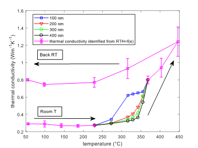
The second method is called the Periodic Pulse photoThermal Radiometry (PPTR) that leads to measure the thermal diffusivity of the PCM layer. All those thermal properties are measured in the 20°C-500°C allowing the different phase changes, from amorphous to different crystalline structures, to occur. As an original result we measured the thermal conductivity of a Ge rich – Ge2Sb2Te5 alloy that is reported in the figure where the phase change occurs at about 350°C.
The main result of BeforeHand related to the material was the assessment of the new golden Ge-rich GST alloy composition, grown by MBE: it turned out to be the best compromise between thermal stability and Ge segregation upon crystallization. The golden Ge-rich GST composition deposited in single devices exhibited better retention and cyclability, and a very low resistance drift, although the resistance contrast is of only one order of magnitude. So such alloy was successfully implemented in the final demonstrator and if the impressive results are confirmed by ST dedicated benchmarking probably further developed in the future by ST Microelectronics.
But it should be underlined that some other remarkable results, related to the other deposition techniques, were obtained in the project, as briefly listed in the following.
The ultra-thin Sb layers (the new frontier of single atomic phase change materials) by PLD turned out to be highly stable at very low thicknesses (3 nm) and the heterostructures containing PLD-grown GaSb sandwiched by Sb2Te3 or Sb exhibited many options to tune the crystallization temperature and kinetics.
The PVD-grown heterostructures containing In-Ge-Te were demonstrated to act as a blocking layer preventing Sb diffusion with a sharp interface.
The sputter-deposited GST alloy could be reproduced in the golden Ge-rich GST composition on both rigid and flexible substrates, paving the way to automotive applications, where large areas and adaptable devices are needed.
An important role was finally played by the MOCVD deposition of 1D heterostructures, namely the core-shell Nanowires; it is worth mentioning that they provided direct access “tools” (especially in the case of Ge-rich GST core NWs with 10 nm thin Sb2Te3 shell), complimentary to the planar heterostructures, to assess the properties of the formed nanointerfaces, whereas Sb2Te3 nanopillars offered the chance to study their positioning in large-area, nanostructured substrates, with the chance to investigate their industrial exploitation for future nanowire-based PCM devices.